Digital to Analog Converters - DAC 2.7 V to 5.5 V, nanoDAC , SPI Interface in LFCSP and SC70
Features:
-
6-lead LFCSP and SC70 packages
-
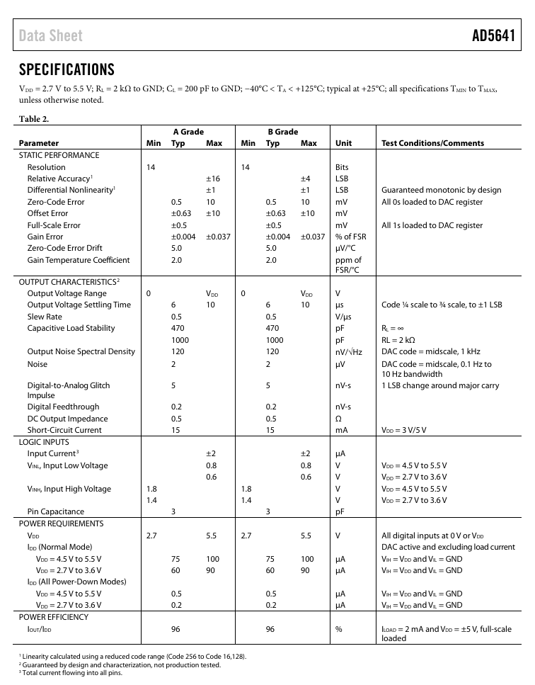
Micropower operation: 100 μA maximum at 5 V
-
Power-down to typically 0.2 μA at 3 V
-
Single 14-bit DAC
-
B version: ±4 LSB INL
-
A version: ±16 LSB INL
-
2.7 V to 5.5 V power supply
-
Guaranteed monotonic by design
-
Power-on reset to 0 V with brownout detection
-
3 power-down functions
-
Low power serial interface with Schmitt-triggered inputs
-
On-chip output buffer amplifier, rail-to-rail operation
-
SYNC interrupt facility
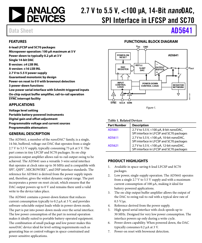
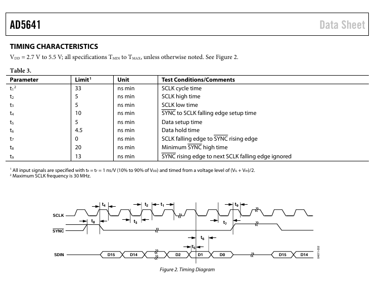
The AD5641, a member of the nanoDAC® family, is a single, 14-bit, buffered, voltage-out DAC that operates from a single 2.7 V to 5.5 V supply, typically consuming 75 μA at 5 V. The part comes in a tiny LFCSP and SC70 packages. Its on-chip precision output amplifier allows rail-to-rail output swing to be achieved. The AD5641 uses a versatile 3-wire serial interface that operates at clock rates up to 30 MHz and is compatible with SPI®, QSPI™, MICROWIRE™, and DSP interface standards. The reference for AD5641 is derived from the power supply inputs and, therefore, gives the widest dynamic output range. The part incorporates a power-on reset circuit, which ensures that the DAC output powers up to 0 V and remains there until a valid write to the device takes place.
The AD5641 contains a power-down feature that reduces current consumption typically to 0.2 μA at 3 V, and provides software-selectable output loads while in power-down mode. The part is put into power-down mode over the serial interface. The low power consumption of the part in normal operation makes it ideally suited to portable battery-operated equipment. The combination of small package and low power makes this nanoDAC device ideal for level-setting requirements such as generating bias or control voltages in space-constrained and power-sensitive applications.
PRODUCT HIGHLIGHTS
-
Available in a space-saving, 6-lead LFCSP and SC70 packages.
-
Low power, single-supply operation. The AD5641 operates from a single 2.7 V to 5.5 V supply and with a maximum current consumption of 100 μA, making it ideal for battery-powered applications.
-
The on-chip output buffer amplifier allows the output of the DAC to swing rail-to-rail with a typical slew rate of 0.5 V/μs.
-
Reference derived from the power supply.
-
High speed serial interface with clock speeds up to 30 MHz. Designed for very low power consumption. The interface powers up only during a write cycle.
-
Power-down capability. When powered down, the DAC typically consumes 0.2 μA at 3 V.
-
Power-on reset with brownout detection.
APPLICATIONS
-
Voltage level setting
-
Portable battery-powered instruments
-
Digital gain and offset adjustment
-
Programmable voltage and current sources
-
Programmable attenuators