Power Management Specialized - PMIC Octal HV digital Pulser
Features:
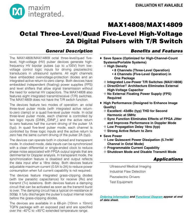
The MAX14808/MAX14809 octal three-level/quad five-level, high-voltage (HV) pulser devices generate high-frequency HV bipolar pulses (up to ±105V) from low-voltage control logic inputs for driving piezoelectric transducers in ultrasound systems. All eight channels have embedded overvoltage-protection diodes and integrated active return-to-zero clamp. Both devices have embedded independent (floating) power supplies (FPS) and level shifters that allow signal transmission without the need for external HV capacitors. The MAX14808 also features eight integrated transmit/receive (T/R) switches. The MAX14809 does not have the T/R switch function.
The devices feature two modes of operation: an octal three-level pulser mode (with integrated active return-to-zero clamp) or a quad five-level pulser mode. In octal three-level pulser mode, each channel is controlled by two logic inputs (DINN_/DINP_) and the active return to zero features half the current driving of the pulser 1A (typ). In quad five-level pulser mode, each channel is controlled by three logic inputs and the active return to zero has the same current driving of the pulser 2A (typ).
The devices can operate both in clocked and transparent mode. In clocked mode, data inputs can be synchronized with a clean differential or single-ended clock to reduce phase noise associated with FPGA output signals that are detrimental for Doppler analysis. In transparent mode, the synchronization feature is disabled and output reflects the data input after a 18ns delay. Both devices feature adjustable maximum current (0.5A to 2A) to reduce power consumption when full current capability is not required.
The devices feature integrated grass-clipping diodes (with low parasitic capacitance) for receive (Rx) and transmit (Tx) isolations. Both devices feature a damping circuit that can be activated as soon as the transmit burst is over. The damping circuit has a typical on-resistance of 500Ω. It fully discharges the pulser's output internal node before the grass-clipping diodes.
The devices are available in a 68-pin (10mm x 10mm) TQFN package with an exposed pad and are specified over the -40°C to +85°C extended temperature range.
Applications