Features
Wide VIN Range: 4.5V to 60V (65V Abs Max)
Wide Output Voltage Range: 0.8V ≤ VOUT ≤ 99% • VIN
Adjustable Gate Drive Level 5V to 10V (OPTI-DRIVE)
No External Bootstrap Diodes Required
Low Operating IQ: 29μA (One Channel On)
Selectable Gate Drive UVLO Thresholds
Out-of-Phase Operation Reduces Required Input Capacitance and Power Supply Induced Noise
Phase-Lockable Frequency: 75kHz to 850kHz
Selectable Continuous, Pulse Skipping or Low Ripple Burst Mode® Operation at Light Loads
Selectable Current Limit (LTC3892/LTC3892-2)
Very Low Dropout Operation: 99% Duty Cycle
Power Good Output Voltage Monitors (LTC3892/LTC3892-2)
Low Shutdown IQ: 3.6μA
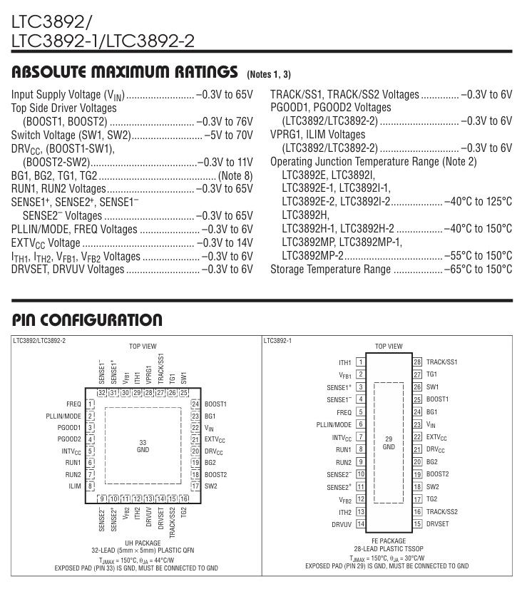
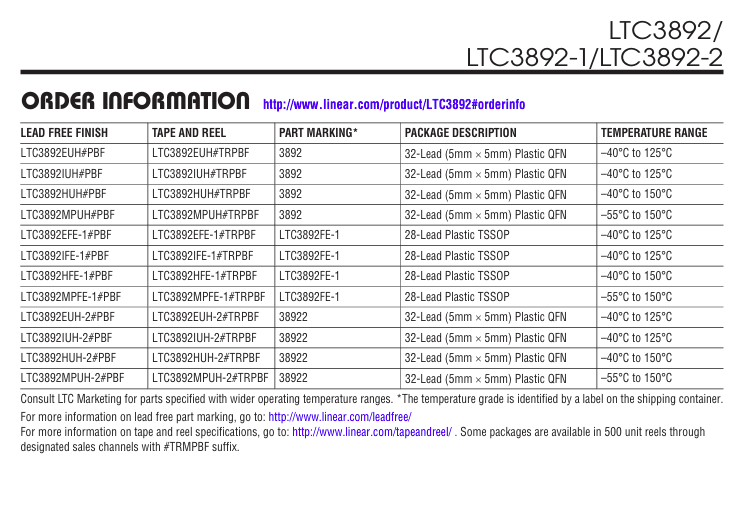
Small 32-Lead 5mm × 5mm QFN Package (LTC3892/LTC3892-2) or TSSOP Package (LTC3892-1)
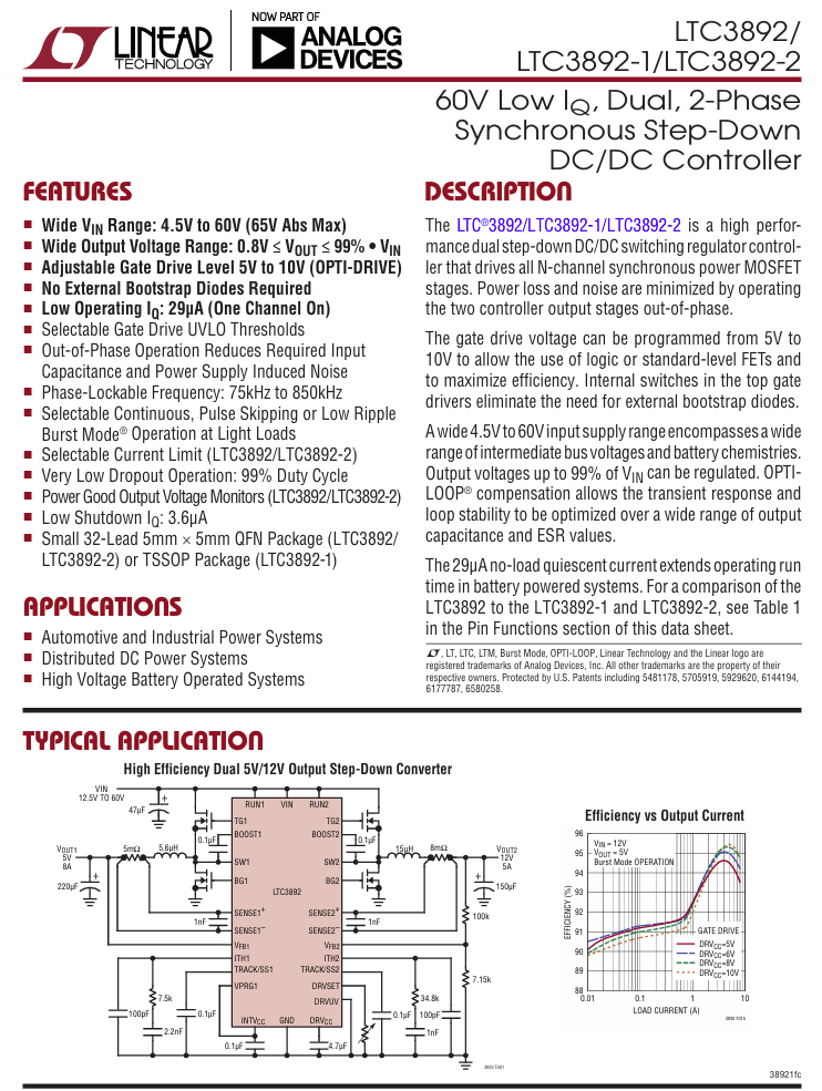
The LTC3892/LTC3892-1/LTC3892-2 is a high performance dual step-down DC/DC switching regulator controller that drives all N-channel synchronous power MOSFET stages. Power loss and noise are minimized by operating the two controller output stages out-of-phase.
The gate drive voltage can be programmed from 5V to 10V to allow the use of logic or standard-level FETs and to maximize efficiency. Internal switches in the top gate drivers eliminate the need for external bootstrap diodes.
A wide 4.5V to 60V input supply range encompasses a wide range of intermediate bus voltages and battery chemistries. Output voltages up to 99% of VIN can be regulated. OPTI-LOOP® compensation allows the transient response and loop stability to be optimized over a wide range of output capacitance and ESR values.
The 29μA no-load quiescent current extends operating run time in battery powered systems.
Applications
Automotive and Industrial Power Systems
Distributed DC Power Systems
High Voltage Battery Operated Systems