Please contact us +852 9724 6575 / sales@youwete.com
Lead (or pin) deformation of electronic components is an extremely common phenomenon during transportation, storage, soldering, or usage. Deformed leads not only affect the normal insertion and soldering quality of components but can also cause circuit short circuits, open circuits, or poor contact in severe cases, thereby impacting the performance and reliability of the entire electronic product. Therefore, mastering scientific and standardized lead correction methods is crucial for personnel involved in electronic manufacturing, repair, and R&D.
I. Common Types and Causes of Lead Deformation
Before discussing correction methods, it is necessary to understand the main types of lead deformation and their causes. Common lead deformations include:
Bending Deformation: The lead bends to one side or at a certain angle, usually caused by external impact, compression, or improper insertion and removal.
Twisting Deformation: The lead rotates along its own axis, mostly caused by improper use of clamping tools or severe vibration during transportation.
Pitch Offset: The spacing between leads of multi-pin components (such as integrated circuits ICs, connectors) changes, possibly due to mold deviation, thermal expansion and contraction, or mechanical stress.
Lead Fracture or Crack: In cases of severe deformation, cracks or even fractures may appear at the root of the lead, often indicating that the component is scrapped.
Poor Coplanarity: The leads of surface-mount devices (SMDs) are not on the same plane, affecting reflow soldering quality.
The main causes of lead deformation include: inadequate packaging protection, vibration and impact during transportation, rough handling by operators, thermal stress during soldering, and material stress relaxation caused by temperature and humidity changes in the storage environment.
II. Basic Principles of Lead Correction
When performing lead correction, the following basic principles must be followed to avoid secondary damage to the components:
Assess Before Operating: Before correction, carefully inspect the component's appearance to confirm whether there are cracks, plating peeling, or internal damage. For leads with cracks or severe deformation, they should be scrapped directly and not forcibly corrected.
Control Force and Angle: Apply uniform and slow force during correction, avoiding sudden force. The bending angle should not be too large; it is usually recommended to adjust in multiple small increments rather than achieving the desired position in one attempt.
Secure the Root: During correction, the root of the lead (close to the component body) must be secured to prevent stress from being transferred to the interior of the package, causing internal wire bonding breakage or chip damage.
Use Appropriate Tools: It is strictly forbidden to use sharp tools (such as tweezer tips, screwdrivers) to directly pry the leads. Dedicated lead correction tools or flat-nose pliers should be used.
ESD Protection and Cleanliness: Anti-static wrist straps must be worn during operation to avoid electrostatic damage to sensitive components; at the same time, keep tools and leads clean to prevent contamination.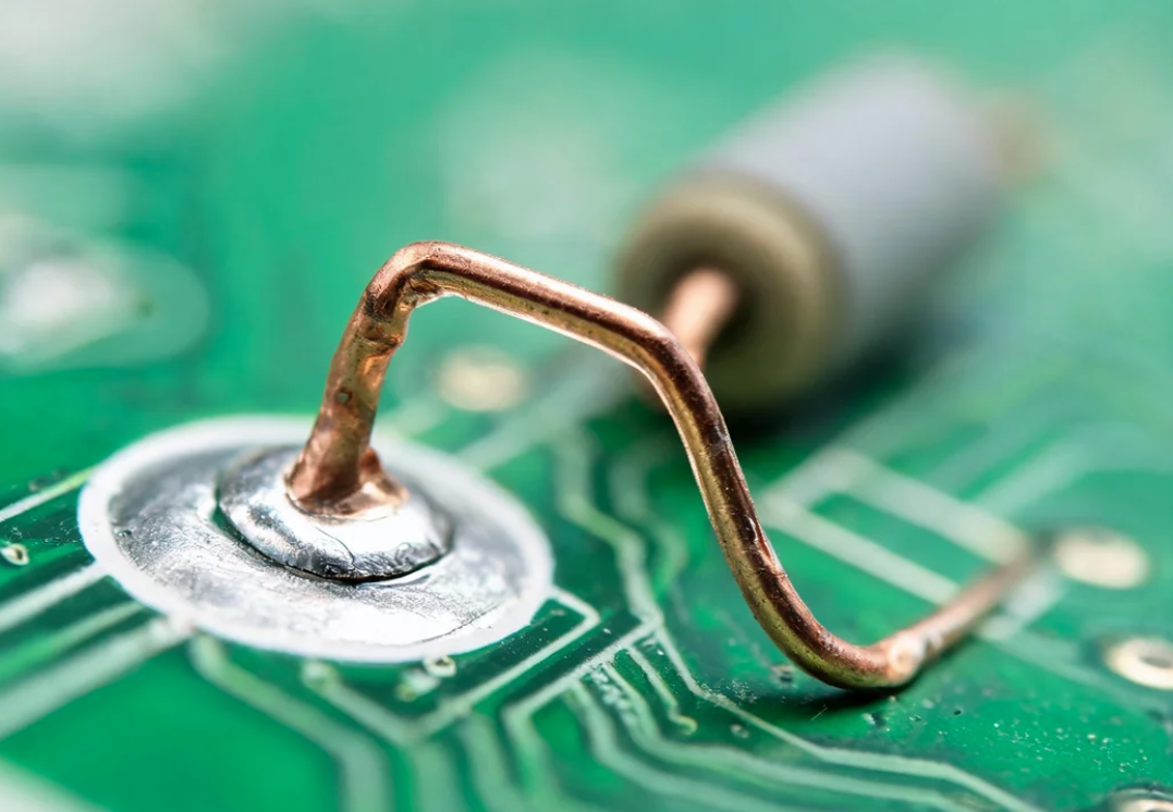
III. Lead Correction Methods for Various Types of Components
(A) Through-Hole Components (DIP, TO Packages, etc.)
Through-hole components (such as DIP packaged integrated circuits, TO-220/TO-3P power devices, resistors, capacitors, etc.) have relatively simple lead correction, but attention must be paid to the standardization of lead pitch.
Correction Steps:
Prepare Tools: Prepare dedicated IC lead correctors (such as PLCC/DIP correctors), flat-nose pliers, rulers, or standard pitch gauges.
Inspect and Position: Place the component on a flat table, observe the lead deformation, and determine which leads need correction.
Secure the Root: Gently secure the root of the lead with fingers or a soft clamp to ensure that the correction force will not be transferred to the interior of the package.
Correct in Stages: For slight bending, gently straighten with fingers; for larger deformations, use flat-nose pliers to clamp the middle of the lead and apply force slowly. It is recommended that each adjustment does not exceed 5 degrees, with multiple fine adjustments to the standard position.
Pitch Verification: Use a standard pitch gauge or IC socket to verify lead pitch, ensuring all leads are parallel and evenly spaced. For DIP packages, the standard pitch is 2.54mm (0.1 inch).
Coplanarity Check: Place the component on a glass plate or flat table to check whether all leads contact the plane simultaneously; if any are lifted, further adjustment is needed.
Precautions: For DIP packages with multiple rows of leads, do not correct multiple leads simultaneously. Handle them one by one to avoid mutual influence.
(B) Surface-Mount Devices (SMDs)
Surface-mount devices (such as QFP, SOP, PLCC, BGA, etc.) have finer and more fragile leads, making correction more difficult and requiring higher precision.
QFP/SOP Package Lead Correction:
Tool Selection: Use dedicated SMD lead correction tools (such as QFP lead correctors, precision tweezers, magnifiers, or microscopes).
Visual Aid: Since lead pitches are small (commonly 0.4mm, 0.5mm, 0.65mm, 0.8mm, 1.0mm), operations must be performed under a magnifier or microscope.
Correct One by One: Use precision tweezers to clamp the upper-middle part of the deformed lead and apply force slowly along the natural extension direction of the lead. For leads that flare outward, gently push inward from the outside; for leads bent inward, gently pry outward from the inside.
Coplanarity Inspection: Use optical inspection equipment or place the component on a flat metal plate and check lead coplanarity using the light transmission method. All leads should be on the same plane, with deviations usually required not to exceed 0.1mm.
BGA Packages: The "leads" of BGA (Ball Grid Array) are actually solder balls. Deformed or detached solder balls generally cannot be manually corrected and require professional BGA rework stations for reballing. If there is only slight offset, the surface tension of the solder can automatically correct it during reflow soldering; if the offset is severe, the component must be removed and re-balled.
(C) Connectors and Headers
Lead deformation of connectors (such as pin headers, female headers, USB interfaces, HDMI interfaces, etc.) often affects insertion/removal functions and electrical connections.
Correction Methods:
Pin Headers/Female Headers: Use small flat-nose pliers or dedicated pin header correction jigs to clamp the middle of the deformed lead one by one and slowly adjust it to a vertical state. For entire rows of offset pins, insert the pin header into a standard socket and apply gentle overall pressure for correction using the socket for positioning.
Board-to-Board Connectors: These connectors have extremely fine leads. Once deformed, it is recommended to replace them directly. Forcible correction can easily lead to lead fracture or loss of contact elasticity.
High-Current Connectors: Such as power interfaces and battery holders, which have thicker leads and can be directly corrected with pliers. However, attention must be paid to plating protection to avoid scratches that may cause oxidation.
(D) Power Devices and Heatsink-Integrated Components
Power devices such as TO-220, TO-247, and TO-3P have thicker leads and are often closely matched with heatsinks, requiring special attention during correction:
Thermal Isolation: If the device has just been removed from the circuit board, wait for it to cool down sufficiently before operating to avoid burns.
Mechanical Strength: These leads have higher mechanical strength and can be directly corrected with pliers, but the root must still be secured.
Heatsink Compatibility: After correction, check the relative position of the leads to the heatsink to ensure that no additional stress is applied during installation.
IV. Introduction to Professional Tools and Equipment
IC Lead Correctors: There are various specifications of DIP/SOP/QFP lead correctors available on the market. Through standard molds, entire rows of leads can be corrected at once, offering high efficiency and consistency.
Precision Tweezers: ESD anti-static tweezers (such as angled tweezers, pointed tweezers) are essential tools for SMD lead correction.
Magnifiers/Microscopes: 5-20x magnifiers or stereo microscopes are used to observe the condition of fine leads.
X-Ray Inspection Equipment: For invisible solder joints such as BGAs, X-Ray can detect internal lead or solder ball deformation.
Coplanarity Testers: Automatically measure the coplanarity of all leads and provide quantitative data, suitable for high-precision requirements.
V. Inspection and Testing After Correction
After lead correction is completed, strict inspection must be carried out to ensure that the component can be used normally:
Visual Inspection: Under sufficient light (or using a magnifier), check whether leads have cracks, scratches, plating peeling, and whether leads are parallel and evenly spaced.
Dimensional Verification: Use calipers or standard gauges to measure lead pitch and length to ensure compliance with packaging standards.
Insertion Test: Insert the component into a standard socket or PCB hole to check whether it is smooth and whether there is any sticking. For SMD components, a "dry" alignment test can be performed by placing them on solder pads.
Electrical Testing: For high-reliability applications, continuity tests and insulation resistance tests should be performed after correction. Functional testing should be conducted if necessary to ensure that the interior has not been damaged by mechanical stress.
Reliability Assessment: For critical components, temperature cycling or vibration testing is recommended to verify long-term reliability after correction.
VI. Measures to Prevent Lead Deformation
Rather than correcting after deformation occurs, it is better to prevent it beforehand. The following measures can effectively reduce the occurrence of lead deformation:
Improve Packaging: Use tube packaging, trays, or tape and reel packaging to prevent components from colliding with each other during transportation.
Standardize Operations: Establish and implement ESD protection and operating procedures, strictly prohibiting throwing or stacking components.
Tool Standardization: Use dedicated insertion and removal tools, avoiding the use of screwdrivers or other substitute tools to pry components.
Storage Environment: Maintain constant temperature and humidity storage to avoid drastic changes in temperature and humidity that may cause material stress changes.
Incoming Quality Control (IQC): Strengthen incoming inspection, and promptly return or screen batches with excessive deformation.
VII. Conclusion
Lead correction of electronic components is a task requiring patience, meticulousness, and professional skills. Different types of components and different degrees of deformation require different correction strategies and tools. The core points are: assess first, secure the root, adjust in stages, use appropriate tools, and close the loop with inspection. For high-value, high-reliability components, if deformation is severe or correction quality cannot be ensured, the most prudent approach is still to replace the component with a new one to avoid potential reliability risks. As electronic components continue to develop toward miniaturization and high density, the difficulty of lead correction is also increasing. Operators must continuously improve their skills and utilize professional equipment to ensure the quality and reliability of electronic manufacturing and repair.